
The fabrication of semiconductor devices involves a series of intricate processes, including lithography, deposition, and etching.
The process begins with the deposition of a thin layer of silicon dioxide on a silicon wafer. Following this, a layer of photoresist is applied to the silicon dioxide surface. This photoresist is then exposed to ultraviolet light through a photomask, which outlines the pattern for the device.
Once the photoresist has been developed, the areas of silicon dioxide that were exposed to the light are etched away through a chemical process, resulting in a patterned layer of silicon dioxide remaining on the silicon wafer.
The next step involves the deposition of a dopant material onto the silicon wafer, typically achieved through a technique known as ion implantation. In this process, the wafer is bombarded with ions of the chosen dopant material.
After the dopant layer is applied, the wafer undergoes a heating process called annealing. This high-temperature treatment facilitates the diffusion of dopant atoms into the silicon, thereby imparting the desired electrical characteristics.
Finally, a series of additional lithography, deposition, and etching steps are performed to construct the various layers and structures that comprise the final semiconductor device. These steps are repeated several times to fabricate complex devices with multiple layers and intricate geometries.
 100% |  Global |  97% | |
|---|---|---|---|
Professional Tutors | International Tuition | Independent School Entrance Success | |
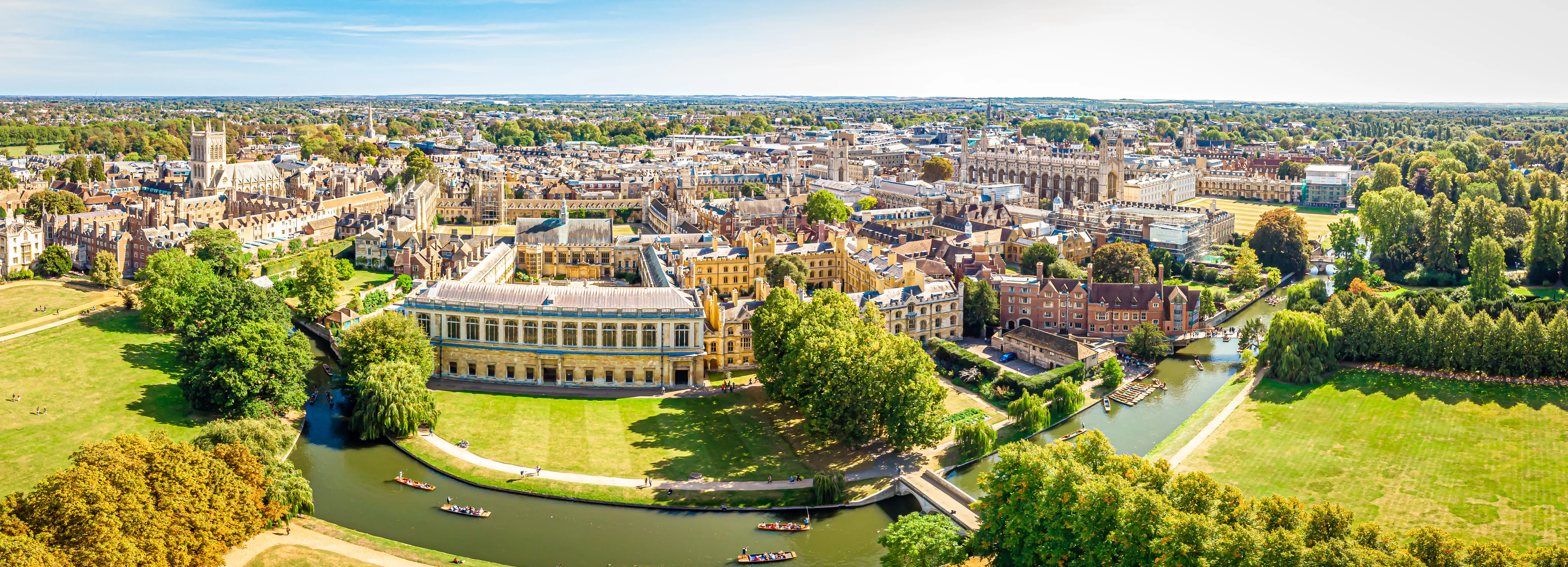
| All of our elite tutors are full-time professionals, with at least five years of tuition experience and over 5000 accrued teaching hours in their subject. | Based in Cambridge, with operations spanning the globe, we can provide our services to support your family anywhere. | Our families consistently gain offers from at least one of their target schools, including Eton, Harrow, Wellington and Wycombe Abbey. |
 100% |
|---|
Professional Tutors |
| All of our elite tutors are full-time professionals, with at least five years of tuition experience and over 5000 accrued teaching hours in their subject. |
 Global |
International Tuition |
| Based in Cambridge, with operations spanning the globe, we can provide our services to support your family anywhere. |
 97% |
Independent School Entrance Success |
| Our families consistently gain offers from at least one of their target schools, including Eton, Harrow, Wellington and Wycombe Abbey. |
At the Beyond Tutors we recognise that no two students are the same.
That’s why we’ve transcended the traditional online tutoring model of cookie-cutter solutions to intricate educational problems. Instead, we devise a bespoke tutoring plan for each individual student, to support you on your path to academic success.
To help us understand your unique educational needs, we provide a free 30-minute consultation with one of our founding partners, so we can devise the tutoring plan that’s right for you.
To ensure we can best prepare for this consultation, we ask you to fill out the short form below.